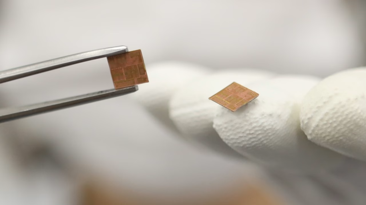
The Microscopic Revolution: How LG Innotek's Copper Post Technology is Reshaping Smartphone Design
It's a constant race, isn't it? Every year, we expect our smartphones to be thinner, lighter, more powerful, and somehow, cooler to the touch, even when they're running demanding apps or crunching AI tasks. For years, the industry has pushed the boundaries of what's possible, often hitting physical limits that seemed insurmountable. But what if a seemingly minor change at the microscopic level could unlock a whole new dimension of design freedom? Well, LG Innotek thinks they've found just that with their new Copper Post packaging technology.
This isn't just some incremental tweak. We're talking about a fundamental shift in how semiconductor substrates – the very foundations upon which our phone's brains sit – are built. And honestly, it’s pretty fascinating when you dig into the details.
Unpacking Copper Post: A Deeper Dive into the Technology
So, what exactly is Copper Post technology? At its core, it's about replacing the traditional solder balls that connect the semiconductor chip to its substrate with tiny, rigid copper pillars. Think of it like this: imagine you're building a multi-story building. Historically, we've used squishy, somewhat malleable "solder pillows" to connect each floor. They work, sure, but they take up space, they're not the best at conducting heat, and you can only stack so many before things get wobbly.
Now, picture LG Innotek coming along and saying, "Hey, what if we use solid, precisely engineered copper posts instead?" These copper posts are much more stable, they can be made incredibly thin, and they're excellent at transferring both electrical signals and heat. This isn't just a material swap; it's a structural re-engineering of the interconnects. And it makes a world of difference.
From Solder Balls to Copper Pillars: The Technical Edge
The traditional ball grid array (BGA) packaging relies on solder balls, which, while effective, have inherent limitations. They require a certain amount of space to form and maintain their shape, contributing to the overall thickness of the package. Copper posts, on the other hand, are fabricated directly onto the substrate, allowing for much finer pitches (the distance between connections) and significantly reduced height.
This vertical efficiency is a game-changer. It means you can pack more connections into a smaller area, leading to denser circuit designs. More connections, more data pathways, more complex chips – all within a smaller footprint. It’s a win-win, really.
The Triple Threat: Slimmer, Denser, Cooler Designs
The immediate benefits of this shift are quite clear, and they directly address some of the biggest challenges in modern smartphone design.
Enabling Ultra-Slim Profiles
The most obvious advantage is the ability to create slimmer devices. By replacing those relatively bulky solder balls with thin copper posts, LG Innotek can reduce the overall height of the semiconductor package. In a world where every millimeter counts, this is huge. Manufacturers are constantly competing to shave off fractions of a millimeter, and this technology offers a tangible way to do just that without compromising performance. Imagine a phone that feels even more impossibly thin in your hand. It's not just about aesthetics; it frees up precious internal space for other components, like larger batteries or more advanced camera modules.
Boosting Packaging Density
Beyond just slimness, Copper Post technology allows for significantly higher packaging density. Because the copper pillars can be made much smaller and placed closer together than solder balls, more input/output (I/O) connections can be crammed into the same area. This means more complex chips with more transistors and features can be integrated into a single package, or multiple chips can be integrated more tightly. This is crucial for high-performance applications and the increasing complexity of smartphone System-on-Chips (SoCs). It's like going from a sprawling suburban layout to a dense, efficient urban grid.
Superior Thermal Management
Perhaps one of the most underrated, yet critical, benefits is improved thermal management. Copper is a far better thermal conductor than solder. This means heat generated by the powerful processors inside our phones can be dissipated more efficiently. Why does this matter? Well, a cooler chip performs better and lasts longer. It also means less thermal throttling – that annoying slowdown your phone experiences when it gets too hot. With AI capabilities becoming more prevalent, demanding intense computational loads, keeping things cool isn't just a luxury; it's a necessity. This could lead to sustained peak performance, even during extended gaming sessions or heavy video editing.
Industry Implications and the Road Ahead
LG Innotek isn't shy about their confidence in this technology. They've already begun mass production, which tells us this isn't just a lab experiment; it's ready for prime time. The company's CEO, Moon Hyuksoo, even suggested it could "change the industry paradigm." Bold words, but perhaps not unfounded. They've also secured a substantial patent portfolio, which is always a good sign of a company's commitment and belief in their innovation.
This move could very well set a new standard for semiconductor packaging in mobile devices. Other manufacturers will likely need to follow suit or develop their own alternatives to remain competitive in the miniaturization race. While the initial focus is on smartphones, it's not a stretch to imagine this technology finding its way into other compact, high-performance electronics, like wearables, IoT devices, or even specialized computing modules. The demand for smaller, more powerful, and cooler components isn't going away anytime soon.
Of course, like any new technology, there will be challenges. Manufacturing at scale with such precision isn't trivial, and there's always the question of cost. But if the benefits truly outweigh these hurdles, and LG Innotek seems to think they do, then we might just be on the cusp of another significant leap in mobile technology. It's exciting to think about what kind of devices this microscopic revolution will enable next.
