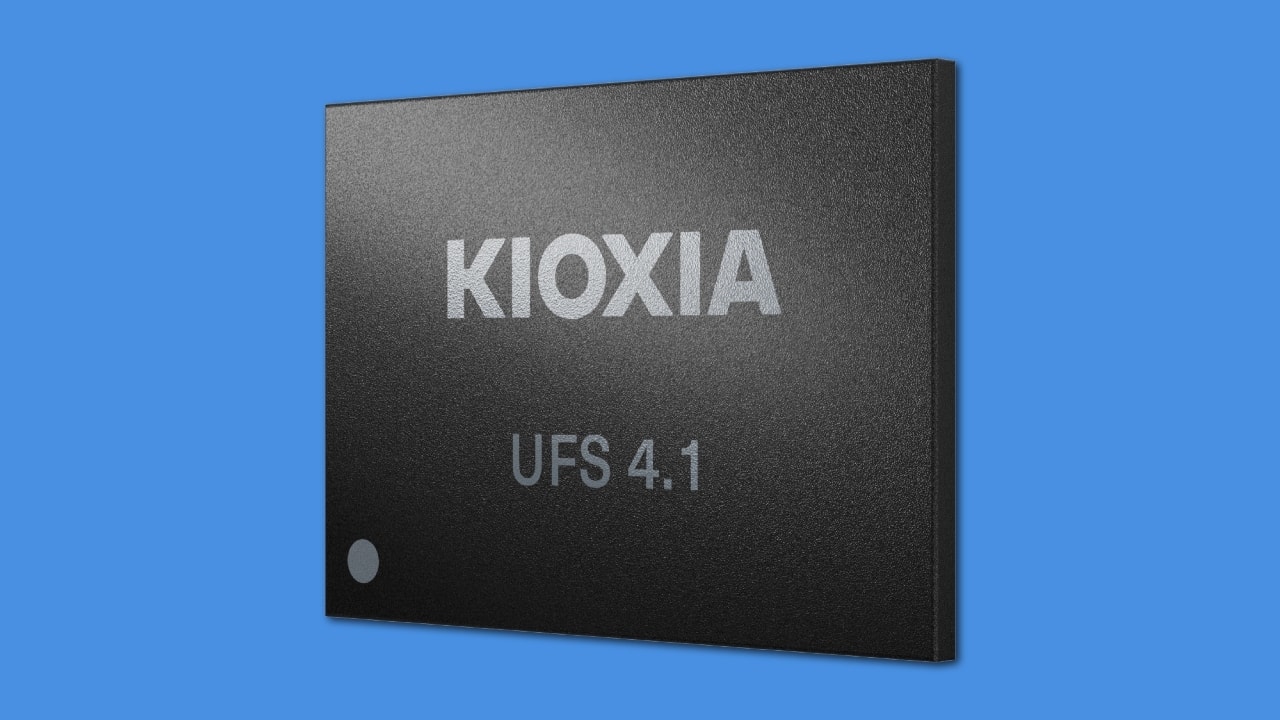
KIOXIA Proves QLC Isn’t a Dirty Word for Flagship Phones
For years, high-end smartphone users have viewed Quadruple-Level Cell (QLC) storage with a healthy dose of skepticism. The trade-off was always clear: you got more gigabytes for your dollar, but you paid for it with sluggish write speeds and a shorter lifespan compared to Triple-Level Cell (TLC) alternatives. KIOXIA is now betting that its latest UFS 4.1 sampling marks the end of that compromise.
By utilizing 8th-generation BiCS FLASH, KIOXIA is pushing 4-bit-per-cell technology into the flagship territory usually reserved for TLC. This isn't just about cramming a terabyte into a phone; it’s a necessary response to the storage-heavy demands of on-device generative AI and 8K video capture—use cases where performance bottlenecks are immediately visible to the user.
Erasing the Speed Penalty
The performance gap between QLC and TLC has historically been a chasm. KIOXIA’s new UFS 4.1 modules aim to bridge it. Compared to the previous BiCS6-based QLC generation, these new units deliver a 25% increase in sequential write speeds.
The real story, however, is in the random access metrics. Random read speeds have jumped 90%, while random writes have nearly doubled with a 95% increase. These aren't just vanity metrics for spec sheets. In a 2026 mobile landscape where "AI Agents" constantly swap small data packets between memory and storage, random write performance is the difference between a fluid interface and a device that hitches under load.
Performance Gains at a Glance
| Metric | Improvement (vs. Previous Gen) |
|---|---|
| Random Write Speed | +95% |
| Random Read Speed | +90% |
| Sequential Write Speed | +25% |
| Write Amplification Factor | 3.5x Better Efficiency |
The CBA Challenge: Why This Architecture Matters
The gains here stem from KIOXIA’s CMOS-directly-Bonded-to-Array (CBA) architecture. In typical NAND manufacturing, the logic (the "brains") and the memory cells are often built on the same wafer or stacked in ways that limit throughput.
CBA flips this. KIOXIA manufactures the CMOS circuitry and the memory array on separate wafers and then bonds them together. This is a massive manufacturing hurdle; aligning two different wafers with nanometer precision requires incredible thermal management and lithographic accuracy. The payoff is a much higher bit density and a shorter, faster electrical path between the controller and the flash cells. This architecture allows KIOXIA to stay competitive with Samsung and Micron, who are also racing to solve the density-performance puzzle.
Solving the Durability Problem (Or Mitigating It)
We have to talk about the elephant in the room: durability. QLC’s four-bit-per-cell structure is inherently harder on the hardware than TLC. Every write cycle puts more stress on the microscopic oxide layers.
KIOXIA is countering this physics problem with a significantly improved Write Amplification Factor (WAF). By optimizing how the controller handles data—specifically through WriteBooster extensions like Pinned Partial Flush Mode—they’ve improved WAF by up to 3.5 times when WriteBooster is disabled.
Is QLC as immortal as TLC? No. But with these overhead improvements, the storage will likely outlive the phone's battery or screen, making the "durability gap" a non-issue for the average flagship buyer.
Can QLC Finally Win the High-End?
The mobile market has reached a tipping point. As of early 2026, 512GB is the floor for high-end devices, and 1TB is becoming the standard. Manufacturers are desperate for high-capacity modules that don't eat up precious internal real estate or kill the bill of materials.
KIOXIA’s UFS 4.1 provides a seamless upgrade path for OEMs, maintaining backward compatibility with UFS 4.0 and 3.1. While the industry still treats TLC as the "gold standard" for pure endurance, KIOXIA’s latest sampling suggests that for the AI-heavy, 8K-recording future, QLC is no longer a budget-tier compromise—it’s the only way to scale.
